|
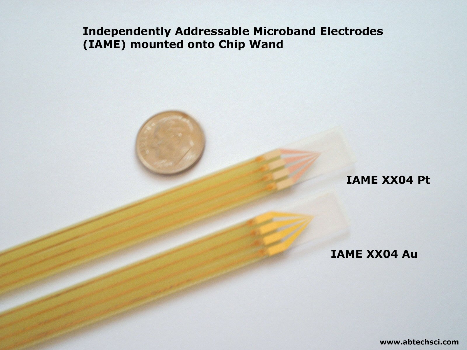
INTERDIGITATED
MICROSENSOR ELECTRODESTM
(IMEs) |
|
View animated
GIF of: |
|
|
|
|
|
|
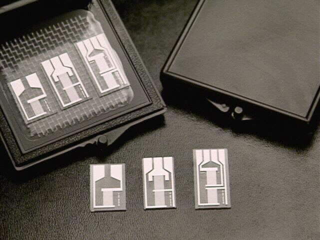
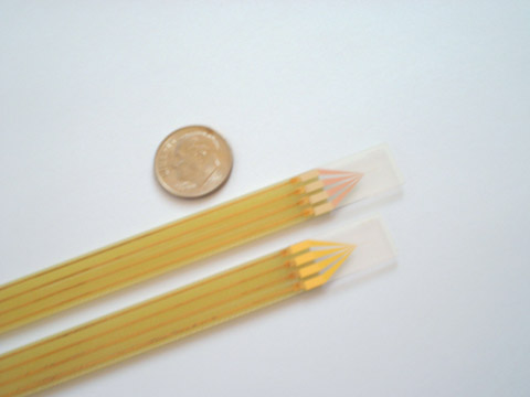
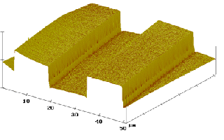
IME DEVICES |
Line and Space, Digit Length |
Designs |
Chip Size (l x w x t) |
Conductor |
|
XX50 Series (50 digit pairs) |
|
|
|
|
|
IME 2050.5 SERIES |
20 microns, 5 mm long |
M |
2.0
cm x 1.0 cm x 0.05 cm |
Au, Pt, ITO |
|
IME 1550.5 SERIES |
15 microns, 5 mm long |
M, CD, FD |
2.0
cm x 1.0 cm x 0.05 cm |
Au, Pt, ITO |
|
IME 1050.5 SERIES |
10 microns, 5 mm long |
M, CD, FD |
2.0
cm x 1.0 cm x 0.05 cm |
Au, Pt, ITO |
|
IME 0550.5 SERIES |
5 microns, 5 mm long |
M, CD, FD |
2.0
cm x 1.0 cm x 0.05 cm |
Au, Pt, ITO |
|
XX25 Series (25 digit pairs) |
|
|
|
|
|
IME 2025.3 SERIES |
20 microns, 3 mm long |
M, FD |
1.0
cm x 0.5 cm x 0.05 cm, |
Au, Pt, ITO |
|
IME 1525.3 SERIES |
15 microns, 3 mm long |
M, FD |
1.0
cm x 0.5 cm x 0.05 cm, 2.0 cm x 1.0 cm x 0.05 cm |
Au, Pt, ITO |
|
IME 1025.3 SERIES |
10 microns, 3 mm long |
M, FD |
1.0
cm x 0.5 cm x 0.05 cm, 2.0 cm x 1.0 cm x 0.05 cm |
Au, Pt, ITO |
|
IME 0525.3 SERIES |
5 microns, 3 mm long |
M, FD |
1.0
cm x 0.5 cm x 0.05 cm, 2.0 cm x 1.0 cm x 0.05 cm |
Au, Pt, ITO |
|
||||||||||
|
Ø Chip Substrate: |
Schott D263 Borosilicate Glass |
|||||||||
|
Dielectric Constant, Epsilon(r) at 1 MHz |
6.7 |
|||||||||
|
Dielectric Loss Angle, tan delta, at 1 MHz |
61 x 10-4 |
|||||||||
|
Electrical Resistivity (50 Hz) (250 C) |
1.6 x 10^8 ohm cm |
|||||||||
|
Coefficient of Linear Thermal Expansion, * 20-300 Deg C |
7.2 x 10^-6 K^-1 |
|||||||||
|
Refractive Index at 20 C, ne ( Lambda = 546.1 nm) |
1.5249 |
|||||||||
|
|
|
|||||||||
|
Ø Metallization: |
100 Å Ti|W / 1000 Å Au or Pt and ITO = 10 Ohms/sq |
|||||||||
|
|
|
|||||||||
|
Ø XX50 Series |
2050.5 |
1550.5 |
1050.5 |
0550.5 |
||||||
|
Digit length, d, (microns) |
4,980 |
4,985 |
4,990 |
4,995 |
||||||
|
No.of digit pairs per sensor, N |
50 |
50 |
50 |
50 |
||||||
|
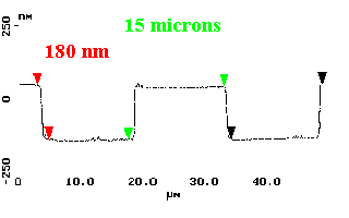
Digit Width, a, (microns) |
20 |
15 |
10 |
05 |
||||||
|
Interdigit Space, a, (microns) |
20 |
15 |
10 |
05 |
||||||
|
Spatial Periodicity, lambda, (microns) |
80 |
60 |
40 |
20 |
||||||
|
Zaretsky Meander Length, M, (cm) |
24.90 |
24.93 |
24.95 |
24.98 |
||||||
|
Center Line or Serpentine Length (cm) |
49.70 |
49.65 |
49.60 |
49.55 |
||||||
|
Cell Constant (cm^-1) |
0.040 |
0.040 |
0.040 |
0.040 |
||||||
|
Ø XX25 Series |
2025.3 |
1525.3 |
1025.3 |
0525.3 |
||||||
|
Digit length, d, (microns) |
2,980 |
2,985 |
2,990 |
2,995 |
||||||
|
No. of digit pairs per sensor, N |
25 |
25 |
25 |
25 |
||||||
|
Digit Width, a, (microns) |
20 |
15 |
10 |
05 |
||||||
|
Interdigit Space, a, (microns) |
20 |
15 |
10 |
05 |
||||||
|
Spatial Periodicity, lambda, (microns) |
80 |
60 |
50 |
20 |
||||||
|
Zaretsky Meander Length, M, (cm) |
7.45 |
7.46 |
7.48 |
7.49 |
||||||
|
Center Line or Serpentine Length (cm) |
14.8 |
14.77 |
14.75 |
14.73 |
||||||
|
Cell Constant (cm^-1) |
0.040 |
0.040 |
0.040 |
0.040 |
||||||
|
Ø IME Chip Dimensions |
Un-packaged Die |
Packaged Die |
||||||||
|
(l x w x t) |
(l x w x t) |
|||||||||
|
M, CD, FD |
2.00 x 1.00 x 0.05 cm |
13.2 x 1.38 x 0.7 cm |
||||||||
|
XX25.3 M |
1.00 x 0.50 x 0.05 cm |
N.A. |
||||||||
|
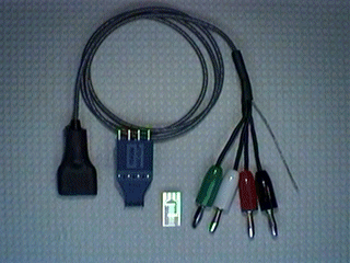
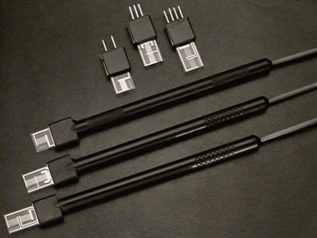
Ø Packaging |
||||||||||
|
Electrode Body: |
PVC-Jacketed printed circuit board |
|||||||||
|
Encapsulant: |
Epoxy header. Polyimide packaged chip. |
|||||||||
|
Leadwires: |
Color coded, 28 AWG stranded copper, shielded, and PVC jacketed |
|||||||||
Back to Top |
||||||||||