PLANAR METAL AND ITO ELECTRODEST(PMES AND PITOES)
(Gold, Platinum and ITO)


PLANAR ELECTRODE PRODUCTS

Critical Dimensions

Designs

Conductor

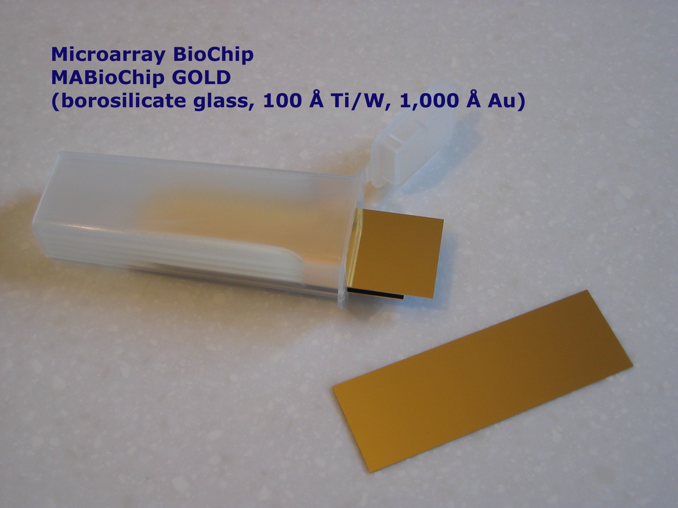
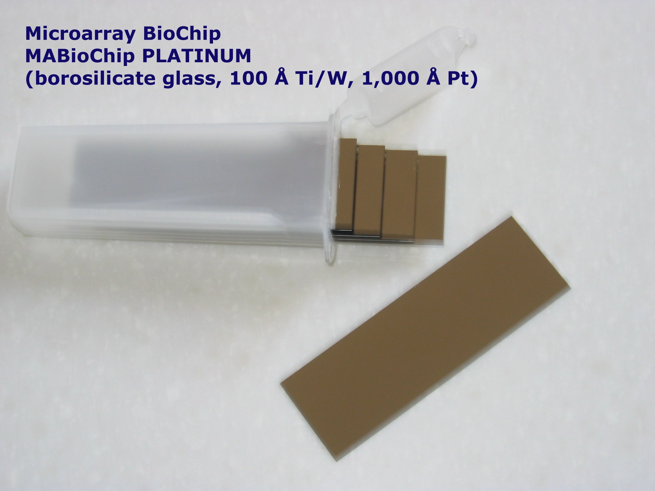
PMEMA1x3AU Microarray BioChip Substrate

1.0” x 3.0” x 0.04”
(2.54 cm x 7.62 cm x 0.10 cm)

Package of 5

BSGlass | 100Á Ti/W | 1,000Á Au

PMEMA1x3PT Microarray BioChip Substrate

1.0” x 3.0” x 0.04”
(2.54 cm x 7.62 cm x 0.10 cm)


BSGlass | 100Á Ti/W | 1,000Á Pt

PME Au 118

1.0 cm x 2.0 cm x 0.05 cm

Package of 6

BSGlass | 100Á Ti/W | 1,000Á Au

PME Au 118-P (packaged chip)

1.0 cm x 1.0 cm x 0.05 cm

1 each

BSGlass | 100Á Ti/W | 1,000Á Au

PME Au 218

2.0 cm x 2.0 cm x 0.05 cm

Package of 4

BSGlass | 100Á Ti/W | 1,000Á Au

PME Pt 118

1.0 cm x 2.0 cm x 0.05 cm

Package of 6

BSGlass | 100Á Ti/W | 1,000Á Pt

PME Pt 118-P (packaged chip)

1.0 cm x 1.0 cm x 0.05 cm

1 each

BSGlass | 100Á Ti/W | 1,000Á Pt

PME Pt 218

2.0 cm x 2.0 cm x 0.05 cm

Package of 4

BSGlass | 100Á Ti/W | 1,000Á Pt

PITOE 118

1.0 cm x 2.0 cm x 0.05 cm

Package of 6

BSGlass | 1,000Á ITO (10 Ohms/p)

PITOE 118-P (packaged chip)

1.0 cm x 1.0 cm x 0.05 cm

1 each

BSGlass | 1,000Á ITO (10 Ohms/p)

PITOE 218

2.0 cm x 2.0 cm x 0.05 cm

Package of 4

BSGlass | 1,000Á ITO (10 Ohms/p)

PITOE 150

0.9 cm x 5.0 cm x 0.05 cm

Package of 6

BSGlass | 1,000Á ITO (10 Ohms/p)

PITOE 150-P (packaged chip)

0.9 cm x 5.0 cm x 0.05 cm

1 each

BSGlass | 1,000Á ITO (10 Ohms/p)

PITOE 250

2.0 cm x 5.0 cm x 0.05 cm

Package of 4

BSGlass | 1,000Á ITO (10 Ohms/p)

PE CUSTOM

YOUR DIMENSIONS

YOUR QUANTITY

YOUR SUBSTRATE

Introduction and Background

Applications of PMEs and PITOEs

Technical Specifications

PME Accessories

Methods

Application Notes

Price List

Introduction and Background

Ø Planar Metal Electrodes (PMEs) are highly uniform thin films of noble metals formed by magnetron sputter deposition or thermal evaporation onto planar insulating glass substrate plates. The conducting layer of gold or platinum (Pt or Au = 1,000 Á) is deposited following deposition of an adhesion promoting layer of titanium-tungsten (Ti/W = 100Á) that serves as the adhesion promoting layer. These layers are deposited onto a very smooth (60/40 scratch and dig finish), highly insulating, chemically resistant and non-leaching, electronics grade borosilicate glass substrate. Substrates such as silicon, with a thermally grown oxide or silicon nitride insulating layer, are also available.
Ø PMEs and PITOEs have plate dimensions of 1.0 cm (w) x 2.0 cm (l) x 0.05 cm (t) (PME 118, PITOE 118) or dimensions of 2.0 cm x 2.0 cm x 0.05 cm (PME 218, PITOE 218). The PME 118 and PITOE 118 are also available as packaged electrodes wherein the chip is mounted onto the WAND CHIP CARRIER and encapsulated with an epoxy resin to reveal an approximately 1.0 cm x 1.0 cm active area.
Ø PMEs and PITOEs may also be supplied in your custom dimensions to meet your uniques research and product development needs. Consult your applications development professional.
Ø PMEs and PITOEs may also be supplied with your custom surface chemistries to meet your uniques research and product development needs. Consult your applications development professional.
Back to top

Applications of PMES and PITOES

Ø Electropolymerization of electroactive polymers:
Ø Reflectance Spectroscopy of ultra thin polymer films and self assembled nano-layers.
Ø Surface modification and derivatization:
Ø Monolayer self assembly of alkane thiol SAMs, Langmuir-Blodgett films, adsorbed protein layers and polyelectrolyte LBL deposition.
Ø Electrodes in electrochemistry.
Back to top

Technical Specifications

Ø Chip Substrate:

Schott D263 Borosilicate Glass

Value

Dielectric Constant, Epsilon(r) at 1 MHz

6.7

Dielectric Loss Angle, tan delta, at 1 MHz

61 x 10-4

Electrical Resistivity (50 Hz) (250 C)

1.6 x 10⁸ ohm cm

Coefficient of Linear Thermal Expansion, * 20-300 Deg C

7.2 x 10^-6 K^-1

Refractive Index at 20 C, ne ( Lambda = 546.1 nm)

1.5249

Ø Metallization:

100 Å Ti|W / 1000 Å Au or Pt and ITO = 10 Ohms/sq

Ø IME Chip Dimensions

Un-packaged Die


(l x w x t)


PME 118 and PITOE 118

1.00 x 2.00 x 0.05 cm


PME 218 and PITOE 218

2.00 x 2.00 x 0.05 cm


Ø Mounting


IME WAND CHIP CARRIER OF PCB


Back to t*op

PME and PITOE Accessories


Perfusion Chamber

CARRIER

Test Clip IME Test Clip

Dimensions

D = 9 mm
V @ 35ml

11.4 cm

N/A

Connector Type

Micropipette

Gold Plated Pins to PCB

Gold Plated Pins

Number of Conductors

2 each chamber: IN & OUT

4 on PCB

4 on one side

Lead

N.A.

N.A.

N.A.

Part No.

PC8R-0.5
Perfusion Chamber

WAND

STC 4

Back to top


Methods

Ø Cleaning: Chips may be cleaned using any of the standard methods developed for microfabricated devices and chips. General advice on cleaning is provided at ABTECH's “Download Files” web page.
Ø Coating: Films or coatings may be applied to the PME or PITOE devices by microcontact printing, dip coating, spin casting, spray painting, air-brushing, brush painting, by the Langmuir-Blodgett thin film deposition technique, by electropolymerization, and by molecular self assembly.
Ø Electrical connection: Electrical connections to the PMEs and PITOEs are best made using the STC 4 Test Clip. Alternatively, you may develop your own method of attachment of leadwires using a conductive epoxy (usually silver), low-temperature micro-soldering (indium) or simple alligator clip.

Back to top


Application Notes

For further information, request Application Notes or you may download application note files:
Ø Because of the many possibilities for the use of PMEs and PITOEs, no application notes have yet been developed in support of this product line.
PME and PITOE are tradenames for a family of devices developed by ABTECH Scientific, Inc. These devices are microfabricated (using microelectronics fabrication techniques) to form patterns of conductors deposited on an insulating substrate chip. They are designed for the simultaneous interrogation of the electrical, electrochemical, and optical properties of thin polymeric films and coatings, for applications in microelectrochemistry, and for electrical/electrochemical impedance spectroscopy.

Back to top


Last Revision 07/24/2005. © 2000-2005 ABTECH Scientific, Inc.

Contact: Ann M. Wilson, Manager,
Applications Development ABTECH Scientific, Inc.
800 East Leigh Street 52, Richmond, Virginia 23219
Telephone Number: +1-804-783-7829 Fax Number: +1-804-783-7830
e-mail: sales@abtechsci.com